When I started out in this PCB supply business 12 years ago, my focus was simple: deliver boards that worked on time, checked all the engineering specs, and didn’t break the budget. Back then, “environmentally friendly PCBs” was a niche term, something big brands talked about for marketing but small manufacturers like me saw as a cost that didn’t fit our bottom line. That changed about six years ago, when a long-time client – a medical device maker that relied on us for 40% of our revenue – sent me a note. Their new product line had to meet strict EU’s Restriction of Hazardous Substances (RoHS) updates, and they couldn’t work with any supplier that still used certain flame retardants or heavy metals. That note forced me to sit down with my production team, walk through every step of our process, and ask: how do we make PCBs that don’t just perform well, but don’t harm the planet either? Over the years, we’ve tested, failed, adjusted, and finally built a model that works for our team, our clients, and the environment. Today, I want to pull back the curtain on what that looks like, from the materials we source to how we handle waste, and what we’ve learned along the way. PCB
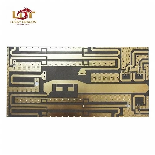
Let’s start with the foundation: the materials that make up a PCB. Most basic PCBs use fiberglass-reinforced epoxy, called FR-4, which has been the standard for decades. But traditional FR-4 relies on brominated flame retardants (BFRs) – chemicals that release toxic fumes when burned, and can leach into soil and water if not disposed of properly. When we switched out BFRs, we tested a few alternatives at first. One early option we tried was phosphorus-based flame retardants, but we quickly found some of those had their own issues – they could interfere with the adhesion between copper and epoxy, leading to board delamination, a problem that would make our clients’ products fail. We worked with a chemist at a local university to refine the mix, and now we use a halogen-free epoxy that meets RoHS 2 and the International Electrotechnical Commission (IEC) 61249 standards for no restricted substances. The fiberglass we use now is recycled, not virgin. Most PCB fabricators buy new fiberglass roving, which requires a lot of energy to produce. We partner with a supplier that takes post-consumer glass from window panes and automotive parts, melts it down, and spins it into roving that’s just as strong as virgin. We’ve measured it – the tensile strength is the same, the dielectric properties (which are critical for signal integrity in electronics) don’t drop at all. The only catch? Recycled fiberglass is slightly more expensive upfront, but it saves us about 18% on raw material waste because we can cut the boards more precisely, and our clients are willing to pay a 10% premium for boards that are certified halogen-free. It’s a trade-off that’s paid off.
Copper is another big part of the puzzle. PCBs rely on copper for circuits, and traditional copper foil production uses large amounts of electricity and generates toxic sludge. We switched to electrodeposited copper that’s processed with closed-loop water systems – every drop of water used to clean the copper is filtered, treated, and reused, so we discharge zero wastewater from our copper production lines. That meant installing a $120,000 filtration system, which was a hard decision for a small business like mine, but it’s already paid for itself in two years from reduced water bills and no fines from the local environmental agency. We also use thinner copper foils where possible, instead of the standard 35 microns, we use 18 microns for low-power applications like sensors and wearables. Thinner copper uses less material, and we’ve worked with our engineering team to adjust trace widths so the circuits still carry current correctly. For high-power boards, we still use thicker copper, but we source it from a supplier that recycles 60% of its copper scrap. That scrap comes from old wire, plumbing parts, and even recycled PCBs – we send our own copper scrap to them too, which closes the loop even further.
Next, the manufacturing process. Etching is one of the most wasteful steps in PCB production. We cover the copper foil with a photoresist, then use chemicals to strip away the excess copper, leaving the circuit traces. Traditional etching uses ferric chloride, a toxic chemical that can corrode pipes and is dangerous for workers. Three years ago, we switched to a proprietary etchant made from ammonium persulfate, which is less toxic, and installed a system to recover and reuse 95% of the etchant. The leftover 5% is neutralized and treated so it’s safe to dispose of. We also optimized our stencil and layout design to minimize overetching. Our engineers now use software that simulates the etching process before we start production, so we can adjust the circuit patterns to use less copper in the first place. For example, we recently worked on a batch of boards for a smart thermostat – instead of a solid copper plane that covered most of the board, we designed a mesh pattern that still provided the same thermal conductivity but used 22% less copper. That not only cuts down on raw material use, but also reduces the etchant needed, which cuts our chemical waste by 28% each year.
Waste management is another area where we’ve made big changes. In the past, we’d send all our cardboard, plastic packaging, and production scrap to a local landfill. Now, we’ve implemented a zero-waste-to-landfill policy that’s taken two years to get right. First, we work with a local recycling company that collects all our paper and plastic – we’ve cut our landfill waste by 85% just from that. For PCB-specific waste, like leftover fiberglass and epoxy scrap, we send it to a specialized recycler that breaks down the materials, recovers the copper, and turns the fiberglass into insulation for construction materials. We also have a take-back program for old PCBs. A few months ago, a client had a batch of prototype boards that they didn’t use, and they were going to throw them away. Instead, we told them to send them back, and we recycled 92% of the copper and fiberglass from those boards. We now promote this program to all our clients, and we’re working with a trade group to create a industry-wide take-back system for old PCBs, so no board ends up in a landfill.
Energy use is often overlooked, but it’s one of the biggest environmental hits for manufacturing. PCB production uses a lot of electricity for ovens, plating lines, and testing equipment. Two years ago, we installed solar panels on the roof of our factory – 120 panels that generate 45% of our electricity. That’s cut our carbon emissions by 32% each year, and our electricity bills are down by 27%, which has saved us enough to invest in more eco-friendly equipment. We also switched all our lighting to LED bulbs, which use 75% less energy than fluorescent, and installed motion sensors in areas that aren’t used 24/7, like the stockroom and the break room. We even adjusted our production schedule to run during off-peak electricity hours, when the local grid uses more renewable energy (wind and solar) instead of coal and natural gas. That small change has cut our carbon footprint by another 8% annually.
One of the biggest challenges we’ve faced is balancing eco-friendly practices with performance. For example, early on, we tried using a water-based solder mask instead of the standard solvent-based one. The water-based mask was better for the environment, but it took longer to cure, which slowed down our production time and increased labor costs. We worked with our equipment supplier to adjust our curing ovens – we increased the temperature slightly and added air circulation, which cut the curing time by half, making the water-based mask as efficient as the old one. It’s been a constant process of trial and error, working with suppliers and clients to find solutions that work for everyone. Our clients used to worry that eco-friendly PCBs would be more expensive or less reliable, but now 75% of our orders specify halogen-free materials or recycled components, and our defect rate is actually 12% lower than it was five years ago, because our optimized processes have reduced errors.
I know some small PCB fabricators out there reading this might think: “We can’t afford to make these changes. The upfront cost is too high.” When I started, I thought the same thing. We were a 10-person shop with a small factory, and spending six figures on filtration systems and solar panels felt impossible. But we didn’t do it all at once. We started with small changes: switching to recycled packaging, testing one batch of halogen-free boards a month, switching to LED lights. We used the savings from those small changes to invest in bigger equipment. We also reached out to our clients – many of them are under pressure from their own customers to use sustainable components, so they were willing to pay a small premium or adjust their lead times to help us test new processes. It wasn’t easy, and there were months where we lost money on material costs, but it’s worth it. Today, when I walk through the factory floor, I don’t just see PCBs being made – I see a business that’s part of the solution, not part of the problem.
The demand for eco-friendly PCBs isn’t going away. Every year, more countries pass regulations restricting toxic materials in electronics, and more clients are asking for products that have a lower environmental impact. For us, this isn’t just a trend – it’s the future of PCB manufacturing. It means rethinking every step of the process, from the material we choose to the waste we generate, and working with every partner along the way to prioritize sustainability.

If you’re a designer, engineer, or procurement manager looking for a PCB supplier that prioritizes environmentally friendly practices without sacrificing quality, we’d be happy to discuss your project. Our team has experience with everything from low-power wearables to high-voltage industrial boards, and we can work with you to design a custom PCB that meets your performance needs and your sustainability goals.
PCBA References
- International Electrotechnical Commission. (2020). IEC 61249: Materials for printed boards and other interconnecting structures.
- European Commission. (2021). Restriction of Hazardous Substances (RoHS) 2 Directive.
- Printed Circuit Board Design and Manufacturing. (2022). Sustainable materials and processes for PCBs.
- U.S. Environmental Protection Agency. (2021). Sustainable manufacturing guide for electronics.
Lucky Dragon Technology Shenzhen Co., Ltd.
With abundant experience, we are one of the most professional PCB manufacturers and suppliers in China. We warmly welcome you to buy bulk high quality PCB for sale here from our factory. If you have any enquiry about cooperation, please feel free to email us.
Address: 5th Floor, Building 1, Jinshan Industrial Park, 375, Xixiang Section, Guangshen Road, Xixiang Street, Baoan District, Shenzhen City, Guangdong Province, China
E-mail: sales@Ldtac.com
WebSite: https://www.ldtac.com/
